
Reverse Engineer Circuit Board
PCB Reverse Engineering
100% accurate and reliable PCB reverse engineering services. We offer fast turnaround time and competitive prices.
PCB Reverse Engineering Service
For PCB reverse engineering, you may send us the below information for evaluation before we get started:
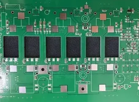
- PCB board two sides picture.
- PCB width and length dimension.
- PCB layers information (if you have)
- Specific requirements if making any changes (silkscreen)
We will provide all the engineering documents (files and drawings) you’ve needed as below;
- Schematic Diagram
- BOM List
- PCB Gerber File
- Pick and Place


What is the PCB Reverse Engineering?
PCB reverse engineering refers to the process of analyzing and understanding the design, layout, and functionality of an existing printed circuit board (PCB) without having access to its original design files or documentation. It involves dismantling or studying the physical PCB and using various techniques to extract information about its circuitry and components.
The purpose of PCB reverse engineering is to gain insight into the inner workings of a PCB, understand its design principles, and potentially replicate or modify it for various purposes.


Benefits of PCB Reverse Engineering
Reproduction
PCB reverse engineering enables the reproduction of a PCB when the original design files or documentation are lost, damaged, or inaccessible.
Repair and Maintenance
PCB reverse engineering aids in repairing and maintaining products for which original design documentation or spare parts are unavailable.
Design Verification and Validation
PCB reverse engineering can be used to verify and validate the design of a product by comparing it against its intended specifications or performance requirements.
Customization and Adaptation
PCB reverse engineering allows for customization and adaptation of existing designs to meet specific requirements or address unique challenges.
Understanding of Existing Designs
PCB reverse engineering enables a deep understanding of existing designs, products, or systems. This knowledge can be valuable for improving or modifying existing designs, identifying flaws, or developing compatible products.
Product Improvement and Innovation
By reverse engineering competitors’ or market-leading products, companies can gain insights into design techniques, manufacturing processes, and technologies used.
How to Reverse Engineering a PCB Step by Step?
PCB reverse engineering is the process of analyzing an existing printed circuit board (PCB) to determine its design and functionality, typically to replicate or modify the board. This process involves a series of steps that require careful attention to detail and specialized tools and techniques. In this article, we will provide an overview of the process of PCB reverse engineering, including the tools and commonly used methods and some of the challenges that may arise during the process.

Step #1: Visual Inspection
The first step is to visually inspect the PCB to identify key components, traces, connectors, and any markings or labels that provide information about the board. This helps in understanding the general layout and structure of the PCB.

Step #2: PCB Imaging
High-resolution imaging techniques, such as optical microscopy or X-ray imaging, are used to capture detailed images of the PCB’s top and bottom layers, component placements, and traces. This helps to understand the PCB’s layout, routing patterns, and component connections.

Step #3: Component Identification
The components on the PCB are identified, including integrated circuits (ICs), resistors, capacitors, connectors, and other active and passive components. This can involve reading component markings, using component databases, or referring to datasheets to gather information about each component.

Step #4: Schematic Extraction
The next step is to extract or create a schematic diagram of the PCB. This involves tracing the connections between components, identifying the circuit elements (such as resistors, capacitors, ICs, etc.), and creating a comprehensive representation of the circuitry. Various techniques may be employed, including manual tracing, signal probing, or using specialized software tools for automated extraction.

Step #5: Picture into PCB file
The TOP layer of the BMP into TOP PCB, pay attention to the transformation to the SILK layer, that is, the yellow layer, and then you trace the line in the TOP layer, and according to the second step of the drawings, place devices. Delete the SILK layer after drawing. Repeat until all the layers are drawn.

Step #6: Comparison of the original board
A laser printer printed TOP LAYER and BOTTOM LAYER to transparent film (1:1 ratio). The film to the PCB, check and modify the correct test of the electronic performance of the copied board is not the same as the original board. The test passes on behalf of the completion of the copy board.

Step #7: Signal Tracing and Analysis
The PCB is analyzed to understand the routing of traces and the arrangement of different layers. This includes identifying power and ground planes, signal paths, and any specific design considerations like impedance control or high-speed signal routing.

Step #8: Documentation and Redesign (if necessary)
Based on the extracted schematic, netlist, and functional analysis, documentation is created to record the reverse-engineered PCB’s details. This documentation can include the schematic diagram, bill of materials (BOM), layout files, and other relevant information. If redesign or modifications are required, they can be implemented based on the reverse-engineered information.
Obsolete or Discontinued Components:
If a critical component used in a PCB becomes obsolete or is no longer available, reverse engineering can be employed to recreate the PCB design using alternative components that are currently available.
Quality Control and Counterfeit Detection:
Reverse engineering can be used to verify the authenticity and quality of PCBs. By comparing a suspected counterfeit PCB to a known genuine PCB, differences in design, component placement, or circuitry can be identified.
Repair and Maintenance:
When a PCB is damaged or malfunctions, reverse engineering can assist in diagnosing the problem, identifying faulty components, and developing a repair strategy. It can also be useful when original schematics or documentation are unavailable.
When Do You Need a PCB Reverse Engineering?
PCB reverse engineering is required in situations where documentation is lacking, components are obsolete, quality control is necessary, design verification is needed, cost optimization is desired, intellectual property protection is sought, repairs or customization are necessary, or when investigating counterfeit products.
PCB Design & PCB Reverse Engineering Services
PCBDesign Lab helped 100 customers develop The Products
Reverse Engineer Circuit Board
Application of PCB Reverse Engineering
Medical Equipment
It helps in troubleshooting faulty devices, identifying design flaws, improving safety and performance, and ensuring compliance with regulatory standards.
Consumer Electronics
It allows companies to analyze and replicate the design of popular products, develop compatible accessories or enhancements, and offer cost-effective alternatives to discontinued or costly devices.

Telecommunications
It analyzes the design of communication equipment, ensuring efficient signal transmission, reducing assembly costs, and improving overall performance.
Renewable Energy
It assists in analyzing and enhancing the electronic components used in solar power systems, wind turbines, and energy storage systems. It helps optimize performance, troubleshoot issues, and improve the overall reliability and efficiency of renewable energy installations.
Reverse Engineering PCB Board
Best Practices for PCB Reverse
Utilization Techniques and Tools
Perform DRC checks to catch the design rule violations
Avoid Auto-Routers
Manual routing can lead to better PCB layouts
3D Scanning and Imaging
Creating accurate digital models of the PCB for further analysis and replication
Documentation and Generation
For future reference and potential replication or improvement of the PCB design

Popular reversing software tools rank
What software needed for PCB reverse engineering?
- Altium Designer
- Protel99
- KiCad
- Auto CAD
- Allegro SPB
- PADS
main features:
- Protel integrates with simulation tools to enable users to validate the reverse-engineered design’s electrical performance.
- Altium Designer, it offers advanced placement and routing capabilities, interactive routing options, and design rule checking (DRC).
- KiCad incorporates a built-in footprint editor that enables users to create or modify component footprints.

Popular reversing hardware tools rank
What hardware needed for PCB reverse engineering?
- Multimeter
- Soldering Iron & Desoldering Tools
- Oscilloscope
- Magnifying Tools
- digital camera
- PCB Cleaning Solution
main features:
- Soldering iron helps remove and replace components without damaging the PCB or surrounding components.
- A multimeter helps in identifying component values, tracing connections, and verifying electrical characteristics.
- A magnifying glass, microscope helps in examining small details, identifying component values, part numbers, and other critical information.
Why Choose US on PCB Reverse Engineering?
Service Capability
- Full ability of 2-10 layers circuit board.
- Component quantity more than 100pcs.
- Sizes within 20 inches.
- We have deeply experienced engineers who have the circuit layout technique by Altium Designer, Cadence, and Kicad.
Price Range
Our service price is from $500-$6000, detailed range as follows for your reference:
- Under 100mm*100mm, 2-4 layers, price approximately $500-$3000.
- Above 100mm*100mm, 6-10 layers, price approximately $3000-$6000.
Files Layout
The sample cannot be used again after we disassembled, and we will convert it as three files for your production.
- Gerber Files.
- Schematic.
- BOM List.
- Pick and Place
Payment Method
We accept direct payment by wire transfer or PayPal.
- Send us the board sample and 50% deposit to start off the project.
- Confirm receipt of the payment and start-up layout files.
- Balance paid before original engineering files are sent.
Shipping Sample Board
Please use DHL or UPS to send us the sample board, and you will be responsible for the tax duty and export clearance charge.
- Please declare the board value at not more than $30 on the shipping invoice.
- Please notify us the tracking number after it is shipped out.
Prototypes Delivery (If you require)
We will use DHL or UPS to send you the prototypes, and you will be responsible for the tax duty or import clearance charges.
- We will declare the prototype value based on the proforma invoice.
- We will notify you of the tracking numbers when they are shipped.
- Customers will be fully charged for the relevant costs of customs duty and customs clearance.
PCB Reverse Engineering: The Service steps you have to know
Project Initiation
The customer initiates the project by providing the existing PCB pictures or samples, along with any available documentation or specifications. Let us know your requirements and objectives for the reverse engineering project.
Physical Analysis
Our team will examine the board layout, component placements, trace routing, and any additional features or structures. This analysis helps in understanding the design and functionality of the PCB.
Schematic Generation
Based on the physical analysis and component identification, our team creates a schematic diagram that represents the electrical connections and relationships between components on the PCB.
PCB Scan Reconstruction
Our team recreates the component placements and trace routing to match the original design as closely as possible. Which is a comprehensive list of all the electrical connections on the PCB.
Design Verification and Testing
This includes design rule checks, electrical rule checks, and simulation tools to ensure the functionality, reliability, and performance of the design.
Documentation and Deliverables
We deliver the reconstructed schematic diagram, BOM list, PCB files, and any additional documentation as required by the customer.
FAQ: All About PCB reverse Engineering
PCB reverse engineering
- Normally, we generate the Gerber file and BOM list and schematic diagram, if you need other format files, like pick and place, pcb file, CAD 3D, please let us know.
- We will check the integrated circuit part number on the board, we only clone the IC without any marked or damaged.
- Yes, we guarantee the schematic circuit and BOM list layout are totally accurate by copying them. Any problems, contact our sales for a resend or revision.
- For the single-layer board with less than 100 components, it takes around five working days to be finished.
- For the multi layers board with more than 100pcs component, it around take up seven working days. It depends on the layers, size and components quantity of the board.
- Yes, we have the PCBA factory partner to manufacture the PCB and source and assembly prototype for you.